Making PCB Pixel Art in Eagle
![]()
What you will need:
- Eagle
- Something to draw art (I use ms paint)
- Built in eagle ulp to import bmp
- Eagle Script to convert layers to specific art layers (can be found at the end of this page or download here)
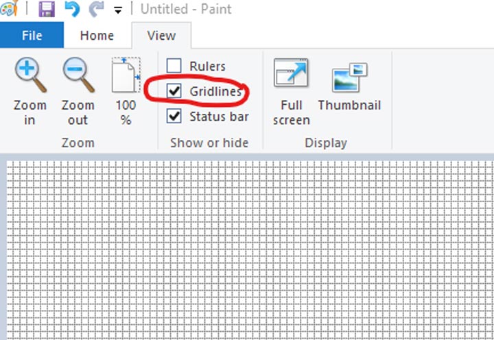
MS Paint Setup
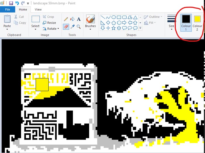
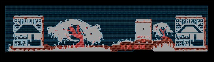
First off you will need to know how big your art will be and how many pixels per mm you will use. I used a pixel/mm size of 4 pixels/mm for my landscape art. At this resolution some of the 1 pixel size silkscreen does not turn out perfect but the other layers like copper and solder mask were fine.
Make note of any things that the art needs to made around. For the stat tracker, the battery icon art had to be placed over the led underneath so you can see the light shine through the FR4.
Make a new paint, resize to your required size and save as a 16 bit colour bitmap. Turn on the grid if you prefer.
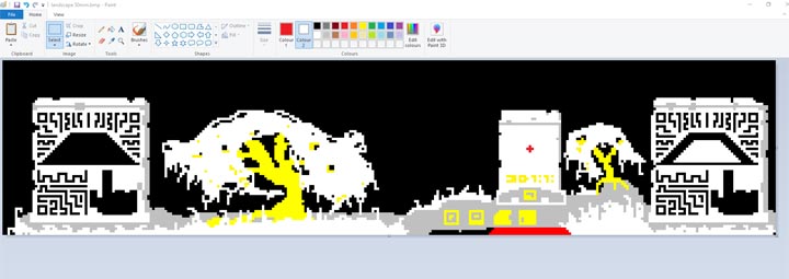
For PCBs you can only do 4 colours. In my case they are:
- (Black) Solder Mask
- (Gold) Copper ENIG
- (Brownish) Exposed FR4
- (White) Silkscreen
You can have different colours based on different soldermask, silkscreen, or copper finishes.
In paint I try to use colours that would be similiar to the final look so it is easier to visualize although you can use whatever colours you wish. The copper layer has the best resolution so use that if you have intricate art.

Use the coordinate system in the bottom left of paint to find out where to put specific art. Don't forget to convert mm to pixels based on your pixel/mm.
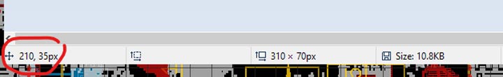
I put important areas in red. The bottom red is the shape the board that will not have art.
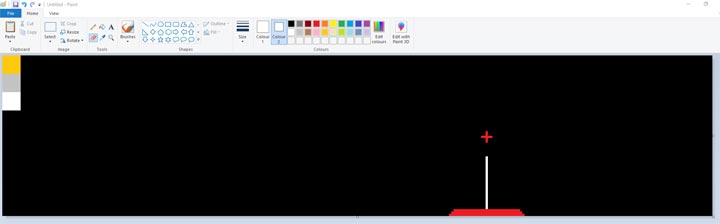
Draw your art
Start drawing!
Colour swap trick
You can use the eraser tool to swap colour 1 with colour 2 using right click.
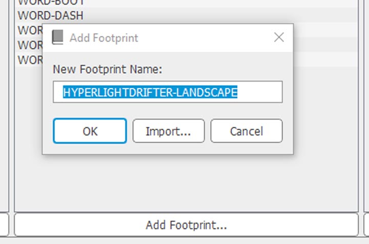
Convert to Eagle part
We now need to make a new eagle footprint which will contain our art. Open up your art library or create a new one. Create a new footprint. I will call mine HYPERLIGHTDRIFTER-LANDSCAPE.
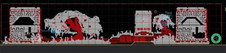
Then run the built in import-bmp ULP. Import your bitmap and select scan used colours.
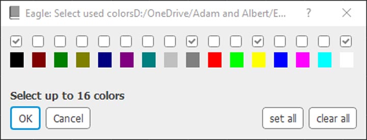
Choose the colours you used in your art.
Select your pixel scale. In my case 1 pixel = 0.25mm.
![]()
Run the generated script. You should see something like this:
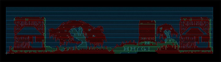
The art has been converted into 4 different eagle layers starting from 200 but we need to convert these layers into the specific copper, soldermask, fr4, and silkscreen layers.
In my case:
- Layer 200 = soldermask
- Layer 201 = FR4 (tstop and trestrict)
- Layer 202 = Copper (tstop and top copper)
- Layer 203 = Silkscreen (tplace)
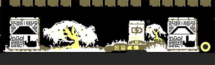
Run the change-art-layers.scr
You should see something like this:
The 200 Layer in blue is left alone because it is the soldermask (in my case) which you do not need to explicitly draw in eagle. Just hide the layer when you are done placing the art.
If the layers are in the wrong area, you may need to adjust the change-art-layers.scr to convert the specific 200 layers to whichever art layer you want.
Save your part and add it to your main board.
If you have eagle 8.6 or newer you can use eagle's built in manufacturing preview on the right side to see the gerber view and confirm that the art looks correct. If not, you will have to generate gerbers and view them in your favourite program. I use ZofZPCB.
The battery icon is a separate part that I placed over white area.
Hopefully this helped you make your own PCB art!
change-art-layers.scr
# use this after importing a bmp to change it into art layers colours (copper silk and fr4)
# find which 200 layers belong to which layers and replace them below.
#
# by Albert Phan 2020


#Silkscreen Layer
#display one layer then convert to tplace
DISPLAY NONE ?? 203;
group all;
change layer tplace (>0 0);

#Copper layer
#Copy layer twice to do tstop and top copper
DISPLAY NONE ?? 202;
GROUP all;
CUT (C>0 0);
PASTE (0 0);
change layer tstop (>0 0);
DISPLAY ?? -tstop;
group all ;
change layer top (>0 0);

#FR4 layer
#Copy layer twice to do tstop and trestrict
DISPLAY NONE ?? 201;
GROUP all;
CUT (C>0 0);
PASTE (0 0);
change layer tstop (>0 0);
DISPLAY ?? -tstop;
group all ;
change layer trestrict (>0 0);

DISPLAY ALL;